
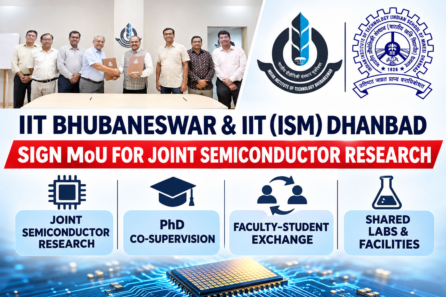
IIT Bhubaneswar and IIT (ISM) Dhanbad sign MoU for joint semiconductor research, PhD co-supervision, faculty–student exchange and shared labs and facilities.
A strategic alliance for semiconductor and basic sciences
Two premier technical institutions, IIT Bhubaneswar and IIT (ISM) Dhanbad, have entered into a memorandum of understanding aimed at strengthening joint research and academic exchange, with semiconductor technology and basic sciences chosen as the first areas of work. IIT Bhubaneswar Director Shreepad Karmalkar and IIT (ISM) Dhanbad Director Sukumar Mishra put their signatures to the document on Wednesday (16 September 2026).
Under its terms, the institutes will run research programmes and projects together, share supervision of PhD scholars and send faculty members and students to each other’s campuses. This collaboration positions both IITs to pool complementary strengths in materials, devices, circuits, systems and foundational sciences critical to the semiconductor value chain.
Joint research programmes and shared supervision
The MoU enables the two institutes to design and execute joint research programmes in semiconductor technology and related basic sciences. Faculty from both sides can co-lead projects on device physics, process technology, packaging, testing, circuit design and system integration.
They will also share supervision of PhD scholars, allowing students to benefit from dual mentorship, access to diverse labs and exposure to different research cultures. Co-supervised theses can tackle complex problems that require expertise in materials characterisation, fabrication, modelling and validation.
Faculty and student exchange for deeper learning
Both sides will look at creating visiting and adjunct faculty positions, along with student movement for classroom sessions, seminars and observerships. Visiting faculty can teach specialised courses, co-develop curricula and mentor research teams on each campus.
Students can spend short terms at the partner institute to attend advanced lectures, use unique equipment and participate in joint labs. Such exchanges broaden technical horizons and build a shared community of researchers across the two IITs.
Joint grant proposals and shared laboratory resources
The institutes intend to approach outside agencies jointly for research grants and to open up their laboratory resources to one another. By submitting combined proposals to national missions, industry consortia and international funding bodies, they can compete for larger, multi-disciplinary projects.
Shared access to fabrication cleanrooms, device testing setups, materials characterisation tools and circuit design labs reduces duplication and maximises utilisation. Researchers can book time on specialised instruments, run cross-campus experiments and validate results using complementary facilities.
Large experimental facilities and competence building
The arrangement further envisages examining the scope for setting up and jointly operating large experimental facilities, apart from holding discussion meetings to build competence in the identified research fields. Such facilities might include pilot process lines, advanced packaging units, reliability test beds or high-performance computing clusters for device and circuit simulation.
Regular joint seminars, workshops and reading groups can help faculty and students stay current with global advances. These forums also create space to define grand challenges, map roadmaps and align efforts with national semiconductor priorities.
Semiconductors as the first focus area
Work on semiconductors will be taken up at the outset, according to the agreement. This focus aligns with India’s push to build domestic capabilities in chip design, fabrication, packaging and testing. Eastern India, with its growing electronics manufacturing base and talent pool, can benefit from strong research anchors.
IIT Bhubaneswar brings strengths in electronics, computing and systems, while IIT (ISM) Dhanbad contributes expertise in materials, mining, metallurgy and energy. Together, they can address the full stack, from raw materials and substrates to devices, circuits and applications.
Synergies between the two IITs
The collaboration leverages natural synergies. IIT (ISM) Dhanbad’s legacy in earth sciences, materials and process engineering complements IIT Bhubaneswar’s work in VLSI, embedded systems and AI-enabled design. Joint teams can explore wide-bandgap semiconductors, power devices, sensors and heterogeneous integration.
They can also study supply-chain aspects such as critical minerals, refining, wafer production and sustainability. By connecting materials science with device and system engineering, the partnership can produce holistic solutions for industry and society.
Talent development for the semiconductor ecosystem
Beyond research, the MoU supports talent development for India’s semiconductor ecosystem. Co-taught courses, joint certificate programmes and summer schools can train engineers in niche areas such as process integration, yield enhancement, design-for-manufacturability and reliability engineering.
Industry internships, sponsored projects and hackathons can further bridge the gap between academia and production. Graduates from this pipeline can join fabs, design houses, equipment vendors and R&D centres with ready-to-use skills.
Alignment with national missions and industry needs
The partnership aligns with national semiconductor missions that seek to attract fabs, packaging units, design-led manufacturing and R&D centres. By building joint capabilities, the two IITs can position themselves as preferred partners for public and private investments.
They can also collaborate with state governments, PSUs and startups on pilot projects, technology transfer and incubation. Such activities can catalyse regional clusters around Bhubaneswar and Dhanbad, creating jobs and innovation spillovers.
Governance and next steps
Effective governance will determine the collaboration’s success. The institutes can set up a joint steering committee, define priority themes, allocate resources and track milestones. Clear MoUs for each project, IP framework and data-sharing protocols will smooth operations.
In the near term, the teams can launch flagship projects, exchange visiting faculty, admit co-supervised PhD scholars and open lab access. Early wins will build momentum and attract further partners and funding.
Looking ahead
With this MoU, IIT Bhubaneswar and IIT (ISM) Dhanbad take a significant step towards a coordinated semiconductor research ecosystem. By combining strengths in materials, devices, circuits and systems, they can contribute to India’s self-reliance in chips and electronics.
Over time, this alliance can expand into joint centres of excellence, shared infrastructure and large-scale industry collaborations. The ultimate goal remains clear: to produce world-class research, train exceptional talent and support a resilient semiconductor future for India.
#IITBhubaneswar #IITISMDhanbad #SemiconductorResearch #JointPhD #FacultyExchange #SharedLabs #MaterialsScience #VLSI #NationalSemiconductorMission #EasternIndia
Disclaimer
The information in this article is based on available public sources and official statements as of the time of publication. While we aim for accuracy, we do not guarantee completeness or correctness. We advise readers to verify key details from official sources before making any decisions. The website (iitiimsamvaad.com) is not liable for any loss or damage arising from the use of this content. The authors are also not responsible for any such loss or damage.