
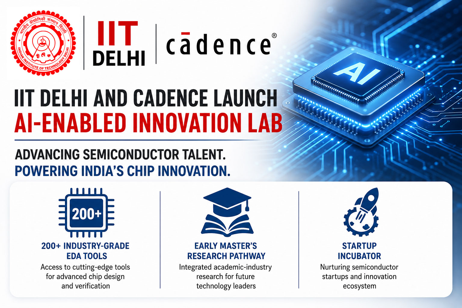
IIT Delhi and Cadence launched AI-enabled Innovation Lab providing 200+ industry-grade EDA tools, Early Master’s Research pathway, and startup incubator for semiconductor talent development.
IIT Delhi-Cadence Innovation Lab Equips Next Generation of Semiconductor Innovators
Cadence and the Indian Institute of Technology Delhi (IIT Delhi) announced the IIT Delhi-Cadence Innovation Lab, a multidisciplinary centre of excellence that equips India’s next generation of semiconductor innovators with the same AI-enabled electronic design automation (EDA) tools and workflows used by industry. The lab advances research, strengthens workforce development and supports pre-seed startups with a streamlined path to first silicon, aligning with India’s Semiconductor Mission and the Design-Linked Incentive (DLI) scheme.
The partnership addresses India’s growing need for skilled semiconductor professionals while providing students access to cutting-edge technology used in professional environments worldwide. This collaboration represents a significant step toward building India’s semiconductor ecosystem and reducing dependency on foreign talent.
Lab Provides Access to 200+ Industry-Grade Cadence Solutions
Providing proven access to 200+ industry-grade Cadence solutions across four domains – chip design verification, digital implementation, analog design and system design and analysis – the lab ensures students, researchers and educators learn on the exact tools used in professional environments. By embedding “design with AI” across these workflows, the lab targets step-change gains in engineering productivity and strengthens the integration of AI in VLSI design.
Students gain hands-on experience with tools that industry professionals use daily, eliminating the learning gap that typically exists when graduates enter semiconductor companies. This direct exposure to industry-grade technology prepares students for immediate contribution to semiconductor design projects.
IIT Delhi adopts Cadence-Developed Courses with Project-Based Learning
IIT Delhi has adopted Cadence-developed courses that combine theory with comprehensive, project-based labs and assessments, moving beyond a theory-only model to hands-on learning with real tools and real-world problem statements. Guest lectures from Cadence and industry practitioners further align learning with current technology roadmaps and career pathways.
The curriculum emphasizes practical application alongside theoretical understanding, ensuring students develop both conceptual knowledge and implementation skills. Industry experts share insights about emerging technologies, career opportunities, and industry expectations, helping students prepare for successful semiconductor careers.
Early Master’s Research Pathway Catalyses Early-Career Exploration
To catalyse research and early-career exploration, the lab is introducing an Early Master’s Research pathway for select fourth-year undergraduates from IITs and NITs, mentored by Cadence experts and IIT Delhi faculty across multiple research areas. This unique programme allows talented students to begin advanced research before completing their undergraduate degrees, accelerating their development as semiconductor innovators.
The mentorship structure combines academic guidance from IIT Delhi faculty with industry expertise from Cadence professionals, providing students with comprehensive support for their research projects. Participants gain exposure to real-world semiconductor challenges while developing innovative solutions.
Incubator Programme Supports Pre-Seed Startups with Low-Cost Tape-Out
In parallel, the lab’s incubator programme supports pre-seed startups on a case-by-case basis with a low-cost route to first tape-out and a working prototype. This support also enables emerging semiconductor companies to validate their designs and develop functional prototypes without bearing the high costs typically associated with chip fabrication.
The incubator programme addresses a critical barrier for semiconductor startups in India, where access to fabrication facilities and expensive tape-out costs often prevent innovative ideas from reaching commercial viability. By providing streamlined access to manufacturing resources, the lab accelerates startup development and contributes to India’s semiconductor innovation ecosystem.
Industry Leaders Highlight Classroom-to-Tapeout Gap Closure
Alok Jain, Corporate VP and India Managing Director at Cadence, said: “Students at IIT Delhi now use the same AI-enabled tools they’ll see on day one in industry, closing the gap from classroom to tapeout. Pairing industry-grade technology with project-based curricula, real-world challenges and targeted startup support strengthens research relevance and workforce readiness for India’s semiconductor future.”
Prof. Jayadeva, Prof. In-Charge of Cadence-IIT Delhi Innovation Lab, stated: “The IIT Delhi-Cadence Innovation Lab combines top-tier academic rigour with cutting-edge industry tools. This partnership will expand research output, prepare students for high-impact careers and help founders move from ideas to prototypes, supporting the goals of the India Semiconductor Mission and the DLI scheme.”
Lab Committed to Increasing Research Output and Graduating Ready Talent
Looking ahead, the Lab is committed to significantly increasing research output, graduating talent ready to contribute on day one, and cementing high-impact collaborations that translate academic innovation into industrial outcomes. The institute aims to establish IIT Delhi as a leading hub for semiconductor research and development while contributing to India’s broader goal of becoming a global semiconductor manufacturing center.
This partnership demonstrates how academic institutions and industry leaders can collaborate effectively to build national capabilities in critical technology domains. The IIT Delhi-Cadence Innovation Lab also represents a model for semiconductor education and innovation that other Indian institutions can replicate to strengthen the country’s semiconductor ecosystem.
#IITDelhi #Cadence #Semiconductor #EDA #VLSI #AIEnabled #InnovationLab #SemiconductorMission #DLIScheme #TalentDevelopment
Disclaimer
The information in this article is based on available public sources and official statements as of the time of publication. While we aim for accuracy, we do not guarantee completeness or correctness. We advise readers to verify key details from official sources before making any decisions. The website (iitiimsamvaad.com) is not liable for any loss or damage arising from the use of this content. The authors are also not responsible for any such loss or damage.